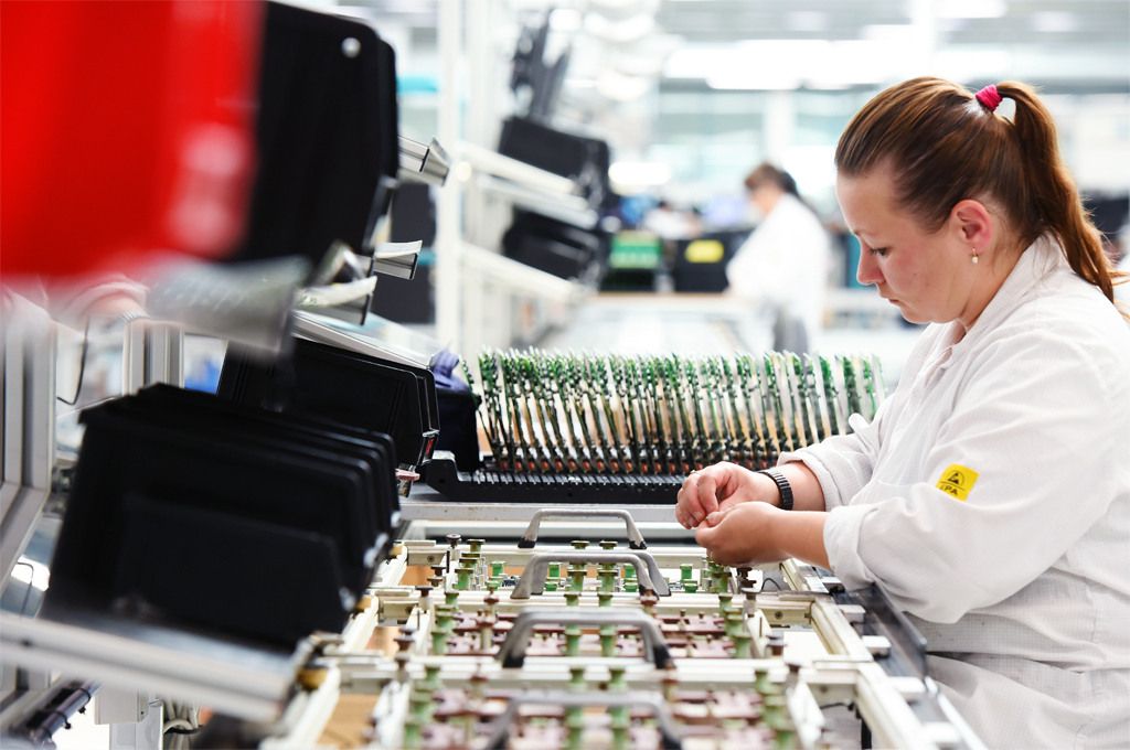
In the intricate world of modern electronics, turnkey pcb assembly (Printed Circuit Boards) stand as the silent architects behind the seamless operation of our devices. These crucial components serve as the backbone of electronic devices, connecting and coordinating the various electronic components, making them integral to the functionality and performance of everything from smartphones and laptops to medical devices and automotive systems. PCB fabrication is a complex and precise process, involving multiple stages of design and manufacturing that demand precision, innovation, and an understanding of the latest technological advancements.
Design: The Blueprint for Functionality
PCB fabrication begins with a detailed design phase. During this stage, engineers and designers create the blueprint for the PCB layout. They consider various factors, including the arrangement of components, the size of the board, the placement of conductive traces, and the number of layers required. Advanced computer-aided design (CAD) software is used to bring the design to life, allowing for a precise and error-free representation of the PCB. The design phase is a critical step, as any flaws or oversights in this stage can lead to costly errors during manufacturing.
Materials and Substrates: The Foundation
The choice of materials and substrates is pivotal in PCB fabrication. The most common substrate material used is FR-4 (Flame Retardant 4), a fiberglass-reinforced epoxy laminate. The substrate provides mechanical support and electrical insulation for the circuitry. The choice of substrate material depends on factors like the intended application, temperature requirements, and cost considerations. Manufacturers may also use specialized materials, such as ceramic, flexible polymers, or metal core boards, depending on the PCB’s unique specifications.
Printing the Layers: Precision in Action
The next step in PCB fabrication involves creating the actual circuitry on the board. This is achieved through a process known as “etching.” Copper sheets are laminated onto the substrate to create conductive layers. A protective layer of photoresist is applied, and the design from the CAD software is used to create a photomask. This photomask is exposed to UV light, creating a pattern on the photoresist. The exposed areas become hardened, while the unexposed areas are removed, leaving behind the circuit’s precise traces. Acid is then used to etch away the unwanted copper, revealing the conductor traces that form the connections between components.